Theme: Pad, soldering point, via, plated-through hole, mounting hole
How can I gold plate pads? E.g. for pushbuttons or for a slot connector?
Various PCB manufacturers offer ENIG ( Electroless Nickel Immersion Gold) as a surface finish. However, this is only a corrosion protection and is intended to improve the solderability of the copper. This is not the point here, but real gold plating.
To do this, you must draw a rectangle or polygon over the tracks and solder points to be gold-plated, e.g. in the gold bottom and/or gold top layer. The copper should therefore be gold-plated in this area. Gold-plated contacts are often used on the edge of the board as plug-in cards / slot cards. As far as we know, the gold is only deposited on the copper, not on the bare FR4 of the circuit board.
You can create slices for buttons in the "gold top" layer across each button (i.e. filled circles). Or, as already mentioned, a filled rectangle over all pads of a slot connector at the edge of the PCB, both at the top and bottom.
Please always discuss this with the PCB manufacturer and mention it again when ordering in writing! The areas can later be exported to an XGerber file as normal.
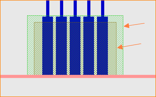
Here is an example for copper at the top only:
 (Fig. 1: Gold-plated contacts on the lower edge of the PCB)
Thick conductor tracks or rectangular SMD pads in the upper copper layer (blue, layer 16). The solder mask is hatched green as a rectangle (layer 18) to keep the contacts free of solder stop varnish and the gold plating is hatched brown (layer 17). Both rectangles are drawn completely over all pads.
Repeat the same for copper bottom on layers 2="Copper bottom", 3="Gold bottom" and 4="Solder mask bottom".