Theme: Pad, soldering point, via, plated-through hole, mounting hole
How can I define "castellated" solder pads on the board edge
"Castellated" solder pads or Plated Half Holes are half-cut plated-through pads on the edge of the board:
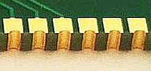 (Image 1: Plated Half Holes)
They are mainly intended to enable a smaller board to be soldered onto a larger one. Several such pads on the edge of the board next to each other make the edge of the board look like a crenellated castle wall. Hence the name "castellated".
To do this, simply place plated-through solder pads with drill hole on layer 100 exactly on the edge of the board. Since the center of the board edge line is what counts, half of each of these vias is milled away after production, creating the solderable hollows.
Some manufacturers require that the PCB remains securely fixed during milling. To achieve this, predetermined breaking points (bridges) are added. In these places, the PCB outline is not milled away, leaving small bridges connecting it to the frame. Outside the PCB, three small drill holes ensure that the PCB can later be easily broken out of the frame.
For example, for the manufacturer Aisler, create a layer with the user-defined function aisler-bridges and draw short lines there near the castellated pads with a width of exactly 0.05588 mm, extending from the outside to just inside the outline:
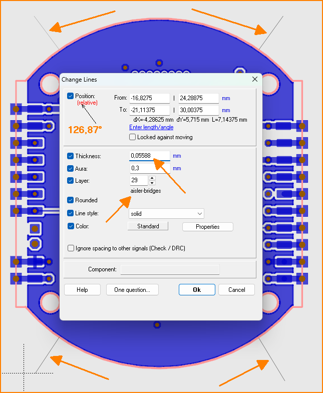 (Fig. 2: For example, four lines for predetermined break points for Aisler)
There should be no other drawing elements or text in this aisler-bridges layer. The lines for these bridges shall be at least 5 mm away from the pads. You can now have your board manufactured with the castellated pads.