Theme: Pad, soldering point, via, plated-through hole, mounting hole
How can I define soldermask or solderpaste independently from the pad shape?
In general the the solderstop mask or solderpaste defines itself by the shape of the pads. You may reduce solderpaste a bit to get a smaller diameter of paste compared to the pad.
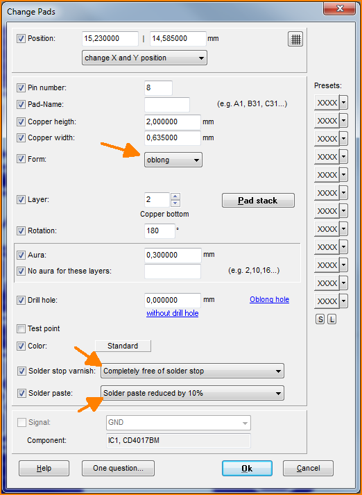 (Image 1: Reduce solder paste
If you need a special arrangement or shape of solder stop or solder paste, please switch off the masking completely in the pad dialog:
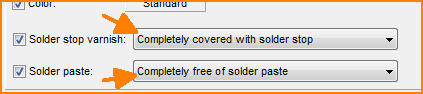 (Image 2: Automatic masking for solderstop and solderpaste switched off)
Now manually draw matching shapes into the designated solderstop and/or solderpaste layer.
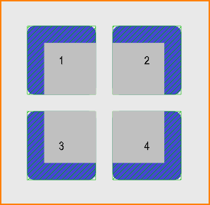 (Image 3: Manually drawn elements on the solderstop and solderpaste layer)
Image 3 shows an "Exposed pad" being placed underneath an IC to dissipate heat. It is devided in 4 copper sections (squares). Each represents a pad on layer 16, copper top in blue. Four squares have been drawn into layer 18, solderstop top, displayed in hatched green. It effects like a mask that no solderstop varnish will be applied here -- which means solderable. Remember that the layers "solderstop" in TARGET 3001! are a mask. All what is displayed green there (or hatched green in this example) later in reality is free from solderstop varnish.
Apart from the center on layer 19, solderpaste, shown in gray there have been drawn four squares. You also might have drawn polygones or filled circles to the layer in question. They represent the solderpaste application.