Theme: PCB outline, shape of the board, copper layers, layers
How can I expand my PCB to 4 copper layers?
Please click on the colored layer stack in the toolbar at the top of the PCB view or use the menu item "View / Layers". In the large layer dialog click on the button [4fold multilayer] on the right:
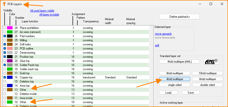 (Fig. 1: PCB layers dialog)
Layers 10 and 13 change from function "Other" to "Copper inside". All solder pads and vias on layer 100 immediately appear on these inner layers as well. You can place traces or add ground planes on these inner layers. It is popular to use the inner layers one as GND and one as VCC, because this creates a capacitor to keep extreme RF spikes away from the supply voltage. This "capacitor" has very low capacitance, but extremely low impedance. It does not replace block capacitors, but supports them in the high frequency range.