How can I adapt a package in the layout after placement? How can I stretch a wired resistor for example?
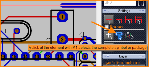
There are many situations where it would be nice to adapt a package in the layout view. In most cases the name and value must be moved and adjusted. But also the length of the leads of a resistor in fact can be angled at any point. So the footprint pattern needs to be adapted accordingly without changing the data in the component database. The most important action is to deactivate the button "Always select housing completely" in the sidebar:
(Image 1: Deactivate the switch to highlight a part always completely if touched anywhere)
Now individual parts ofpackages can be selected and edited. The name and value can now be placed appropriately by dragging and dropping with [M1H]. You can also use [M1H] to move a solder point of a wired resistor or transistor:
(Image 2: Move a pad away from its initial position)
Now the pad is moved away from the body and TARGET asks if you really want to tear the component apart. Yes, of course, that was the idea! So please confirm this dialog with [Yes]. If you like you can also extend the line to the soldering point for a neat look. You then connect the resistor with tracks and you can route under it with many other tracks:
(Image 3: Further tracks underneath the resistor)
Of course, it would be better to do this with both pads, so that the body of the resistor is placed in the middle. You know how it works now. When changing packages, please always remember what is really feasible. If, for example, you want to assemble by automat or you look for a larger series, please contact your assembly house in advance to avoid that your adaptions cause disproportionately high effort.
 (Image 1: Deactivate the switch to highlight a part always completely if touched anywhere)
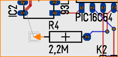 (Image 2: Move a pad away from its initial position)
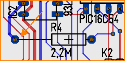 (Image 3: Further tracks underneath the resistor)