One question...

Theme: Package, component in PCB

How do I create an "Exposed Pad" having through holes when creating a component
Some components dissipate heat underneath their body by the use of an "Exposed pad". In most cases it is just a copper rectangle underneath the component. Often additional vias (galvanized through holes) are placed into this copper rectangle in order to dissipate heat towards the other side of the board.
1 
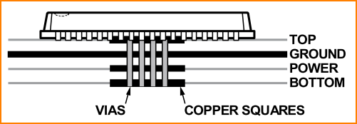
(Image 1: Areas and through holes (vias) in an ADAU1452 by Analog Devices)

It is possible to create such a part by the use of the TARGET- package generator in order to give it the finishing touch (add missing elements) later.
2 
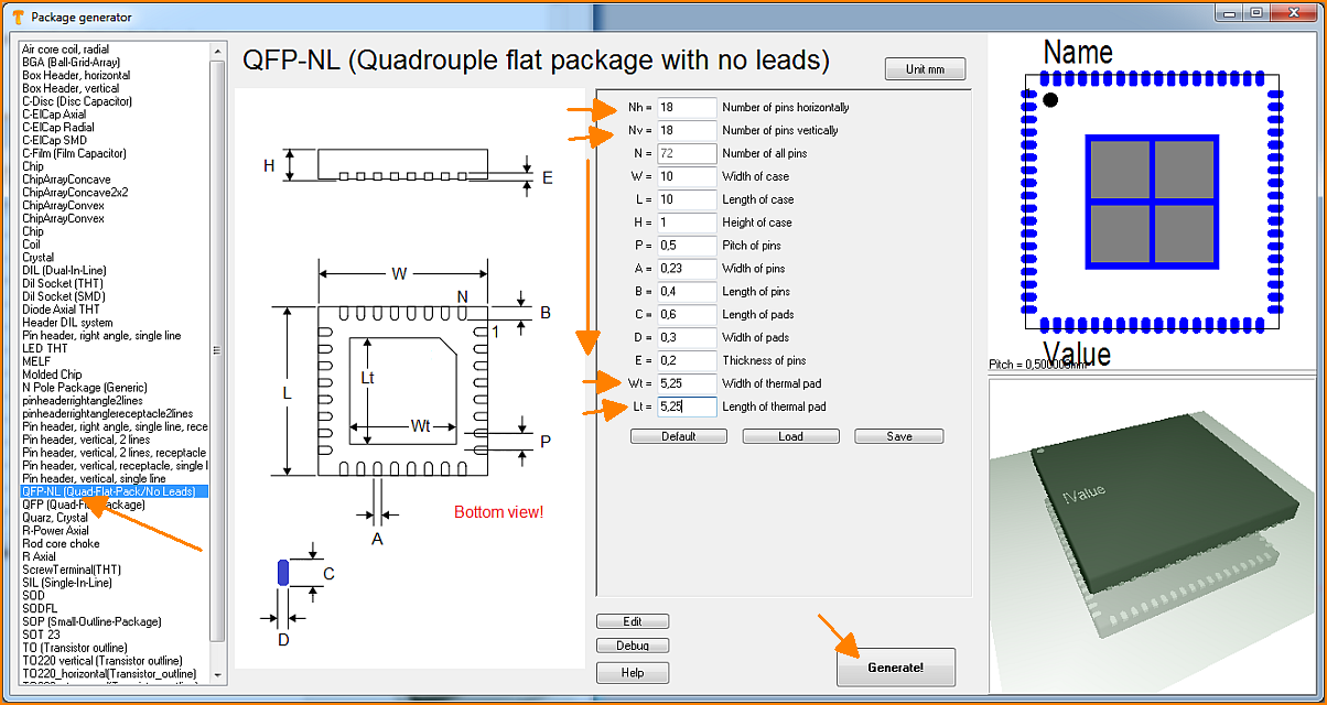
(Image 2: Package generator for a QFP-NL)

Enter all values from the data sheet to the fields and press [Generate]. Now save the part as type QFN using the name LFCSP72 (=as recommended in the the data sheet).
3 
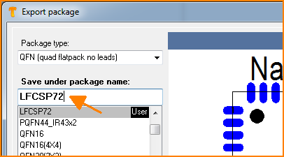
(Image 3: Save with a name as a type)

Now we need to add some amendments because the Generator has created only one inner pad on copper top as exposed pad.

4 
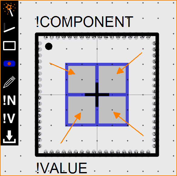
(Image 4: Edit the package)

First we delete the 4 gray rectangles in the solder paste layer. Hover the mouse over each gray rectangle press [s] for select as often until it flashes and press [Del] in order to delete it. You get asked whether you intend to rip the part apart. You say Yes. Now you can delete the little gray square. After you have done this four times, click laterally on the blue inner pad with a double click (in TARGET we call such clicking action "M11").
5 
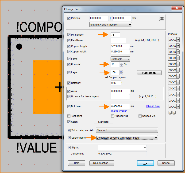
(Image 5: Edit Exposed Pad )

The Pin number remains 73. The corners may slightly get rounded. The layer definitely needs to be set to 100 "All Copper Layers". We set the drill hole to 0.4mm (separate decimals by comma). Important is to have the solder paste covering the pad completely. In the center now we have already one via (= the drill hole). The following vias we also need to define as soldering pads(!) all having Pin number 73. For placing further pads we press keyboard key [1] and then [o] for options.
6 
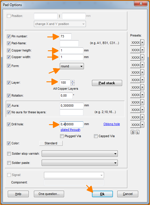
(Image 6: Small vias as pads all with pin number 73)

Now we place the pad once and press [s] for select:
7 
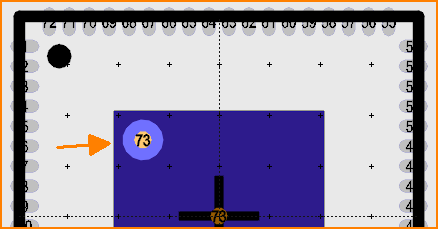
(Image 7: soldering pad selected for use as a via within an exposed pad)

Now click menu item Duplicate in menu Edit in order to 74 further pads into the exposed pad.
8 
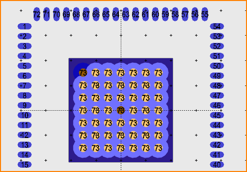
(Image 8: All in all 7x7=49 vias within the square pad, the d?first one above left.)

The package is ready now and we can export it to the data base. Press [Ctrl]+[a] in order to highlight all and hover the cursor to the center (0|0) to define the place for the handle cross.

Press [x] in order to export the package to the data base. TARGET alerts that several pads would have the same Pin number. But that's what we want. We overwrite the generated one by this saving action - Done.